AD9910 sideband noise
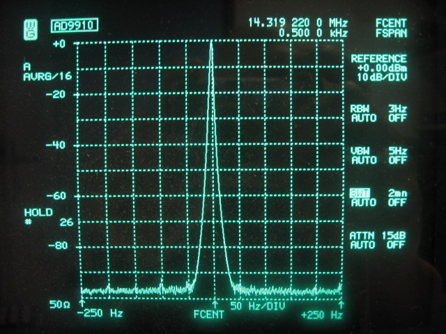
The following analyzer screen shot shows the AD9910 0dBm carrier at 14.319Mhz. With the 3Hz resolution bandwidth of the analyzer, its noise floor is reached at 50Hz away from the carrier. This demonstrates that a general-purpose spectrum analyzer is not good enough to show the noise sidebands of clean signal sources like the AD9910 DDS. The analyzers noise figure is too high and its dynamic range is too limited to be able to do this. Therefore we have to use more specialized phase noise measurement methods.
Given the impressive spur results, or better said the lack of spurs with the AD9910, I was getting convinced that the AD9910 board was a winner! The only thing remaining to be done was to verify that the phase noise performance was close enough to what could be expected from the residual phase noise plots in the AD9910 datasheet. The expectations in the "phase noise department" were pretty high because of the estimated performance of the Wenzel based 1GHz clock source and the residual and absolute phase noise graphs provided by ADI. Furthermore the really low spur levels gave confidence in the double sided PCB layout and the other design choices made with this board.
Reciprocal Mixing Method results
So at this point it was finally time to do some validation of the phase noise of the AD9910 DDS. I don't possess or have access to a sophisticated SSE (Signal Source Analyzer) capable to directly measure the phase noise of the DDS down to the thermal noise floor. Therefore an improvised way of measuring phase noise was needed. One of the methods, which is especially convenient when measuring LO phase in a receiver, is the Reciprocal Mixing Method.
The noise sidebands of the AD9910 DDS prototype board are measured using this method when tuned to 14.318MHz. This frequency is chosen because of the availability of inexpensive standard crystals needed for the crystal filter used in this method. This means that with the IF positioned at 9MHz, the DDS is actually running at 23.318MHz. The results together with the baseline phase noise and the residual noise of the AD9910 at 20.1MHz (from the datasheet) are plotted together in the following graph (scales are in dBc/Hz and KHz):
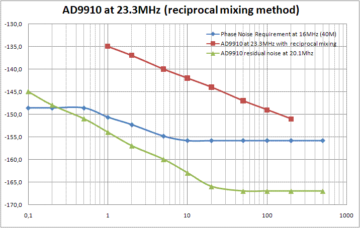
The result, the red series, does not even come close to the required level, the blue series, let alone the maximum achievable plot, the green series. The residual plot and the reciprocal plot are not scaled down to the 16MHz baseline frequency, but that would account only for a 3dB improvement of the reciprocal plot which is clearly not enough! In fact the single sideband noise of the AD9910 is about 20dB stronger than we could theoretically hope for given the residual measurements at 20.1MHz by ADI and also way above the baseline.
The reciprocal mixing method measures single sideband noise including phase noise, when the LO is embedded in the receiver. This means that not only the LO itself is measured, but also the complete signal path from the LO up to the mixer. In my experimental receiver this includes a low noise MMIC amplifier, the 74AC04 based squarer on the frontend board and finally also the FSA3157 switches of the H-Mode mixer. In order to leave these extra factors out of the measurement a different method was needed to drill down further into the problem.
Notch Filter Method results
Another elegant and simple method to measure sideband noise, including phase noise, is the Crystal Notch Filter Method. I implemented this method, inspired by Wes Hayward's, W7ZOI, article "Oscillator Noise Evaluation with a Crystal Notch Filter" in the July/August 2008 issue of QEX. It now became possible to directly measure the single sideband noise of the AD9910 DDS prototype board at 14.318MHz with the spectrum analyzer and the results are shown in the following graph (scales are in dBc/Hz and KHz):
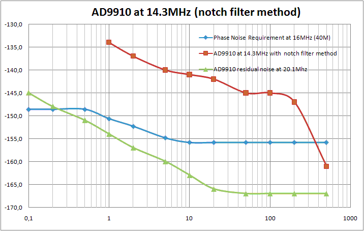
The notch filter method shows rather similar, actually slightly worse results, in comparison with the reciprocal mixing method. Given the lower working frequency of 14.318MHz instead of 23.318MHz, one would have expected better results, with a factor of about 4.2dB in case of phase noise! This is the first indication that we are not dealing with phase noise at all!
The other observation that can be made is that the notch method shows a sudden reduction in the noise level starting about 200KHz away from the carrier and outwards. This is new information. With reciprocal mixing I could only measure up to 200KHz away from the carrier, given the pass-band of the antenna BPF of the receiver. At this point there is quite a bit of evidence that the excessive sideband noise is originating from my AD9910 DDS prototype board, now that the receiver is not part of the measurement system anymore. It also shows that the reciprocal mixing method is working quite well, because the notch filter method confirms its results.
Excess Noise Sources
With the excess noise now confirmed by two entirely different measurement methods it is needed to find the root of the problem. The five main areas to look for the source of the noise are:
-
Reference clock.
-
Power supplies.
-
PCB layout.
-
AD9910 chip revision.
-
AD9910 analog circuits.
Apart from these points, the problem can also be caused by the measurement methods themselves. Although chances are slim when two different methods produce quite similar results, it cannot be ruled out completely. Therefore I put especially the notch method through quite a lot of scrutiny, but nothing wrong could be found. More about that can be found here: Crystal Notch Filter Method
Reference clock
The 100MHz Wenzel oscillator used in the 1GHz reference clock has very good phase noise specs (-155dBc/Hz at 1KHz offset from 100MHz), however I have no means to directly verify the phase noise at the 1GHz output after the 10x frequency multiplication. Therefore, the reference clock is a possible although unlikely suspect of introducing the excess noise measured with the AD9910 prototype board. In order to eliminate the reference clock as the source of the problem the following simple tests have been done:
-
Eliminating the 10x multiplier by clocking the AD9910 directly with the Wenzel at 100MHz.
-
Clocking the AD9910 with a completely different source, a Vectron 500MHz TCXO.
The outcome of these tests is that when clocking the DDS directly with the 100MHz Wenzel OCXO or with the 500MHz Vectron TCXO, there is no significant difference in the measured noise level. The phase noise of the TCXO is unspecified. The unit is only specified for good frequency stability, therefore its phase noise is probably not in the same class as the Wenzel oscillator, but still no difference in the end result. This firmly indicates that the reference clock is not the cause of the excess sideband noise of the DDS.
Power supplies
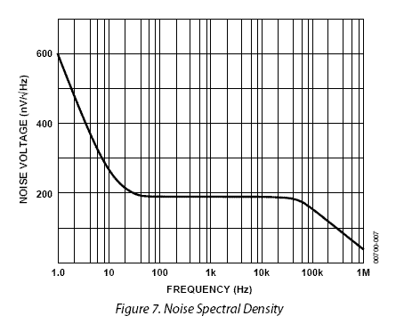
My AD9910 DDS prototype board has 4 onboard LDO voltage regulators for the different power rails of the DDS chip: 1.8V and 3.3V analog, 1.8V and 3.3V digital. It occurred to me that the noise plateau of the AD9910 resembled the noise plots of the LDO regulators! They produce relatively much noise up to a few hundred KHz out and then drop off quickly towards the thermal noise floor. See the following picture grabbed from the datasheet of the MIC5205 LDO regulator that is used with the analog 3.3V supply powering the AD9910 DAC:
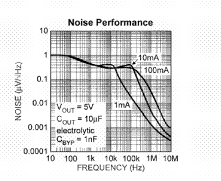
There is a remarkable resemblance with this graph and the observed AD9910 noise plateau! The idea is that the noise of the analog power supplies, especially the 3.3V analog rail, is causing excess noise sidebands on the output signal due to the finite power supply rejection of the AD9910 analog DAC circuits. The Micrel MIC5205 is marketed as "low-noise" LDO although the graph tells that this must be some kind of relative definition of "low-noise".
In order to confirm or eliminate this theory I have designed and build "ultra-low-noise" discrete voltage regulators, because no truly "low-noise" off-the-shelf regulator IC's could be found! The definition of "low-noise" regulator used in that search was that its noise should be expressed in nV/√Hz rather than μV/√Hz and preferably less than 10nV/√Hz. My homebrew regulators are using a band-gap voltage reference that is de-noised with an RC filter cutting off at 0.5Hz. A low noise, wideband opamp is used as the error amplifier with unity closed-loop gain. The noise level of such a voltage regulators is very low, roughly identical to the input noise voltage of the opamp, which in this case is only 4.5nV/√Hz.
I replaced the onboard regulator voltages one by one except 3.3V digital by the ultra low noise supplies. Each time the DDS sideband noise was measured for any changes. There is absolutely no difference of the resulting noise plots within the accuracy of the measurement method (1dB). This result eliminated the noisy power supply theory at least for now.
PCB Layout
It seemed rather unlikely, but maybe also the PCB layout could play a role in the noise especially with the low noise levels we are talking about. My AD9910 prototype board is a simple double sided board. Usually, more expensive 4-layer boards are deployed with such an application, which for sure is more convenient when doing the layout and gives much more freedom in assigning complete layers as power planes and ground planes. To unnerve the PCB-layout theory, I needed a professionally designed and engineered 4-layer board for the AD9910.
What could be a better candidate for this test than ADI's AD9910 Evaluation board? After all, the evaluation board is the very same board that has been used to produce those excellent residual and absolute phase noise plots in the first place with! Once again, it was Colin, G3SBI, and the Daresbury Laboratory connection that could help me out by providing an AD9910 Evaluation board that was available at the Daresbury Lab!
Apart from the AD9910 based DDS, the evaluation board contains a USB microcontroller and comes with an easy to use PC software package to control all details of the AD9910 with a PC. Once the board had arrived in the mail, I could not wait to power it up with my laboratory bench supply and in the next couple of days I repeated all the measurements made earlier on the double sided AD9910 prototype board.
When I designed my 2-layer board I have thoroughly examined the evaluation board gerbers available for download at www.analog.com, in order to use anything that could be learned from those layouts. Therefore I was not too hopeful that the 4-layer evaluation board would behave much better than my 2-layer design. This turned out to be the case. The sideband noise plots measured with the evaluation board were almost overlapping with the earlier measurements. This test scrubbed yet another possibly noisy candidate from the list!
AD9910 chip revision
Suspicion existed regarding the actual DDS chip revision being used on my prototype board, because it is a pre-production chip obtained through the early sample program before the AD9910 was officially released. The evaluation board now at my disposal had a production chip soldered to it. The tests with that board also proved that the pre-production chip is not causing the problem.
AD9910 analog circuits
Arriving at this point the list of possible causes, external to the AD9910 chip, had more or less been exhausted. None of the experiments made so far had shown a significant change in the noise plateau observed with the AD9910. So ADI's DDS design lab was contacted with a detailed report on the AD9910 noise plateau and the effort made so far to find the source of the problem, including full details on the 2 measurement methods. ADI could not explain my results and were not much convinced of the existence of the noise plateau as their sophisticated test equipment did not show it.
But still the similarity between the noise plateaus of the LDO regulator and the AD9910 cannot be ignored. The AD9910 noise has all the signs of a band-gap reference voltage device. The following graph is grabbed from the datasheet of the AD1580 1.2V voltage reference:
It shows a plateau of 200nV/√Hz. That is -135dB relative to the 1.2V DC output voltage. That coincides quite nice with the dBc/Hz values of the plateau observed with the AD9910. Also the cutoff point is at roughly the same offset. That is why Colin, G3SBI, suggested that the internal band-gap device of the AD9910, which is used as the reference voltage to accurately set the DAC bias current, might be the real problem! If the internal band-gap device is not thoroughly filtered, then the noise will end up directly in the output signal of the DAC.
The following experiment is finally the start of a breakthrough in nailing the source of the noise. One of the AD9910 registers, Auxiliary DAC control, is meant to programmatically set the DAC bias current. The DAC bias is defaulted to 20mA with value 127. Programming this value to 0 reduces the bias current to about 8.6mA. Changing the DAC bias current gave finally the so needed significant change in the noise plateau as can be seen in the following picture (scales are in dBc/Hz and KHz):
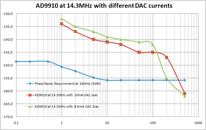
There are two strong effects. First, the plateau comes up consistently by 2 to 4dB's, which is significant. Second, the cutoff frequency offset changes by as much as an octave from 200KHz to 100KHz, which is very significant! This is strong evidence that the AD9910's internal DAC circuit is at the root of the problem!
Now the pieces of the puzzle are finally coming together. All its predecessors like the AD985x and AD995x families of DDS chips have a pin called DACBP, which can be used to decouple the noisy DAC reference voltage by means of an external capacitor. The AD9951 datasheets only explanation of this pin is the statement that it is the "DAC Biasline Decoupling Pin". All DDS chips introduced by ADI in recent years including the high-end 1GHz, 14-bit chips like AD9910, AD9912 and AD9957 do not have the DACBP pin anymore. The reason why ADI did this "optimization" is unclear. But still the evidence is quite convincing that a big capacitor is really needed on a "DACBP" pin to take out the noise plateau caused by the internal band-gap reference of the DAC.
Because it is impossible to test the effect of a decoupling capacitor on the AD9910 by the lack of the very pin, I reverted to the AD9951 to see how much effect the bypass capacitor can give with that device. The following plots are measured with I0CG's AD9951 DDS board using different values of the bypass capacitor. The AD9910 plot is also added for comparison (scales are in dBc/Hz and KHz):
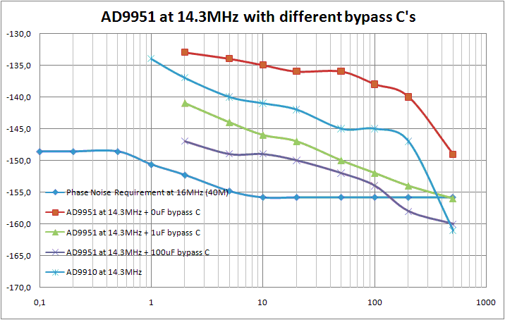
Without the bypass capacitor, the AD9951 is noticeably worse than the AD9910, but it shows the same characteristic plateau effect with a cutoff frequency at an offset of around 200KHz from the carrier. However there is a vast improvement possible when the bypass capacitor is added. With 100μF the AD9951 plot approaches the requirements with about a 5dB distance. That is still not good enough, but it is the best we have seen so far! Furthermore, the noise of the 100μF-bypassed AD9951 DDS could possibly be improved further if the remaining excess noise happens to be caused by the onboard LM317 voltage regulators.
AM-noise versus PM-noise
One of the big questions remaining now is why ADI cannot reproduce the noise plateau that I can measure so easily with two different but simple and reliable methods in my home-lab! ADI had been somewhat reluctant so far to accept my measurements, which is understandable given the reputation of the signal source analyzer from Agilent they use.
At that point I decided to homebrew a simple PM-noise test-set in order to validate the results with yet a third and completely different measurement method: The Quadrature Mixing Method. The mixer method would also allow for much more flexibility like measuring at different frequencies and also much closer-in than was practically possible with both the notch and the reciprocal mixing method. Furthermore, the Agilent SSE also uses the mixing method. While I was busy doing that, ADI was looking together with Agilent into the issue. The mystery was solved quickly when the SSE was configured to measure AM-noise rather than PM-noise. In AM-noise mode the noise plateau finally appeared also on the analyzer display at ADI!
In retrospect this is all rather logical. The Agilent SSE is based on the quadrature mixing method, which by design rejects AM-noise. It really only measures PM-noise. The unfiltered band-gap reference noise however is modulating the DDS signal purely with its amplitude, because it sets the DAC bias current directly! In general PM-noise is much more important than AM-noise. PM-noise cannot be filtered away easily, but AM-noise can be scrubbed of by carefully clipping the carrier with a squarer.
The reciprocal mixing method showed the noise plateau from the start. The reciprocal mixing method evaluates the DDS while it is embedded in the receiver. In that configuration the DDS signal is squared up with the 74AC04 squarer on the frontend board before it drives the FSA3157 H-Mode mixer switches, which at least in theory should have scrubbed of the AM-noise to a large degree. So already from the start, AM-noise was not considered to be an issue at all, which turned out to be a wrong assumption. The reciprocal mixing method and the notch filter method however measure any sideband noise; AM-noise and PM-noise. It is unclear at this moment why the squarer on the frontend board does not seem to sufficiently suppress the AD9910's excess AM-noise. Possibilities are that it converts the AM-noise to PM-noise, or that it introduces AM-noise or PM-noise on its own. This is a subject of a further study that I hope to report on soon!
Is AD9910 broken?
The answer to the question whether it is an insignificant design flaw or a pretty serious one that the AD9910 produces orders of magnitude more AM-noise than its documented PM-noise, depends on the application where the chip is used for. If the chip is used in an application where the AM feature of the AD9910 with the 14-bit ASF register is not used and a sinus wave output signal is unimportant, the answer is probably no, not a serious problem. Just scrub of the AM-noise with a squarer and use the square wave instead of the sinus wave output signal. On the other hand if you really need a clean sinus wave output with or even without 14-bit resolution AM, and excess AM-noise cannot be tolerated, the reality is that then there is a problem. In my opinion, with a DDS chip that has 14-bit amplitude control built-in, AM-noise is an important device parameter and ADI should have documented it completely like is done with PM-noise.
The current state of the AD9910 chip without the DACBP pin blows away for instance the plans to easily improve the 2-tone test generators I use for IMD3 measurements with a better much lower phase noise, much lower spur solution based on the AD9910. I don't need the ASF in that case, but I do need a clean sinus wave output! Of course squaring things up properly and then use 10 or so switchable low pass filters to restore the sinus wave could be done but a simple decoupling capacitor would have been so much simpler!
I have not done any testing with the other 1GHz DDS parts like AD9912 and AD9957 yet. They do not have a DACBP pin either and therefore the expectation that those chips will be better regarding the AM-noise issue is rather low. But at least AD9912 has the on-chip squarers that may be successful in scrubbing the AM-noise off!
Can AD9910 be fixed?
All we can hope for now is a new chip revision of AD9910 with the DACBP pin put back into service! This seems like a relatively simple change to an otherwise great DDS chip. The side of the chip that is related to most of the analog functionality has actually no less than 7 unused pins available in the current chip revision. So the change could even be made in a backward compatible way without invalidating existing designs that don't care so much about the AM-noise. We also hope that ADI's future DDS chips will have the DACBP pin exposed again or even better: if possible, have the AM-noise issue solved internally without the need for an external capacitor.
The answer to the question, can the AD9910 AM-noise issue be easily fixed by ADI, is clearly yes. Whether it will be actually done is something that only ADI can tell! Adding the missing DACBP functionality is a very simple way to improve the current revision. Significant improvements in other areas of the AD9910 however will be much more challenging for the DDS design team, because it is a great chip already! One can think of more bits in the DAC and more GHz in the clock, both of those together would be ideal for the next generation (V)HF-LO DDS!
1GHz Reference Clock
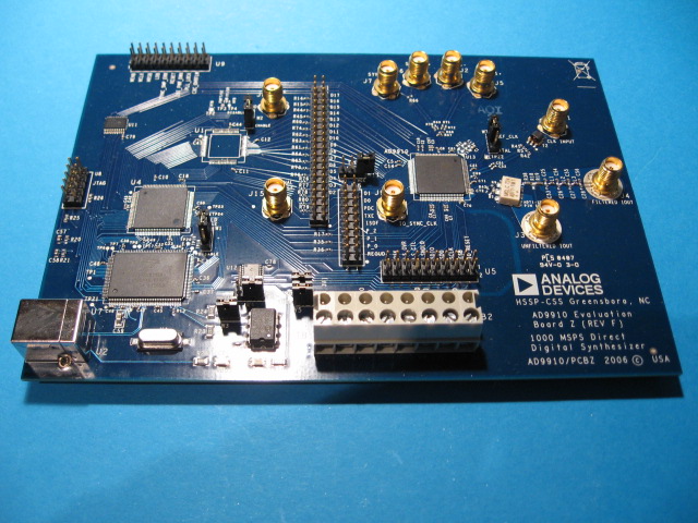
AD9910 Prototype Board
AD9910 and SSB-Noise
AD9910 and PM-Noise
Back to LO Design Choices
Back to the TOC
|